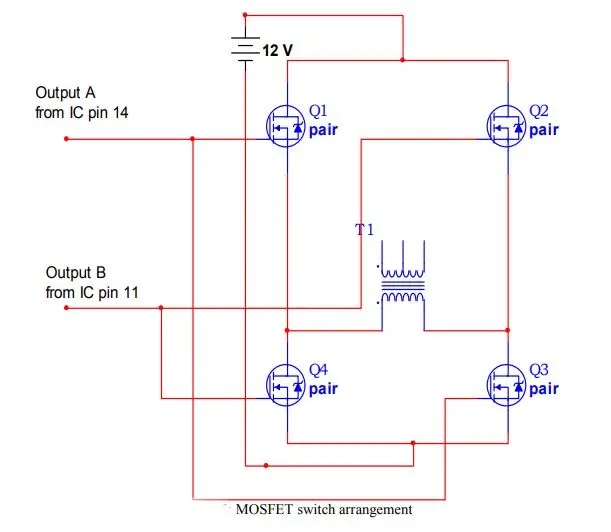
Full bridge power inverter
The main difference between the two configurations is that the output voltage of full bridge inverter is equal to the power supply voltage while output voltage for the half bridge inverter is equal one half of the power supply voltage. Since the output power is proportional to the square of the voltage then the output power of the full bridge will four times of that of the half bridge. This would be enable operation of the amplifier at lower voltage to get the same power which will reduce the size of the battery.
The switching frequency used in this project is 50Hz. It is desired to control the inverter with proper switching signals. The turn on and turn off time of the switches is determined by this PWM control signal generated by the 3525A IC controller. Before this control signal is being generated, proper calculation is done to determine the suitable switching pulses conditions (frequency) for the switches
Figure below shows the approach in which the controller outputs are connected with the inverter MOSFET switches as used in this work. The turn ON and OFF for Q1 and Q3 are controlled by PWM A generated at pin 11. While the turn ON and OFF for Q2 and Q4 are controlled by PWM B generated at pin 14. Both PWM A and PWM B used the same control signal generated by the IC. With PWM A signal leading PWM B by half cycle or 180 degree of the switching signal.
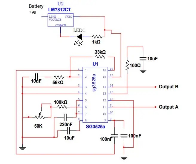
The Controller Circuit using 3525A PWM IC
This serves as the controller. It produces PWM pulses and these pulses are provided to the MOSFET switches such that the MOSFET gates can be triggered ON and OFF. This is responsible for generating oscillating signals that controls the ON and OFF action of the MOSFET switches.
The control circuit as a whole was made with a 3525A PWM IC and combination of some passive components. The oscillation from its output pins is controlled by a timing resistor and capacitor connected to pins 5 and 6 terminal of the IC.
The 3525A is a 16-pin device and included in it are all the control necessary for PWM. They include reference voltage regulator, an error amplifier, a comparator, an oscillator, under-voltage lockout, soft start circuit, and output drivers.
It uses negative feedback to force the voltage at the inverting input (pin 1) of the error amp to be equal to the voltage at the non-inverting input (pin 2) of the error amp. The internal oscillator drives a flip flop. Each half-cycle of the flop puts on the NOR gate for a full PWM cycle. It has an internal pair of complementary BJT gate drivers that deliver high and low output voltages necessary to adequately drive power switches
The soft start circuit is necessary for limiting the pulse width produced when the IC initially starts operating, and the soft-start time is governed by the following relation. t (sec) = CSS x Vout / I
where t is soft-start delay time in seconds CSS is charging capacitor connected to pin 8. In this work 10uF is used as shown in figure 1 to obtain a 0.50 sec delay during turn ON.
Vout is the soft start threshold voltage at which value the inverter starts from the device datasheet, this value is 2.5V max I is the soft-start current as provided by the internal current source in the IC (50uA). It has an under-voltage lockout component which has a threshold at 7V+㆒1V to shut down its output at a voltage below its normal input voltage Vcc range.
The reference regulator supplies all other internal sub circuits of the IC a reference of 5V for operation. The comparator creates PWM signals based on the difference between the internal oscillator signal and the carrier signal which comes from pin 9 and pin8. The IC operates at a voltage range of 8V to 35V.
- Supply voltage Vcc 8V to 35V
- Collector supply voltage Vc 4.5V to 35V
- Oscillator frequency range 100Hz to 400 KHz
- Oscillator Timing Capacitor CT 1nF to 0.2µF
- Oscillator timing Resistor RT 2KΩ to 150kΩ
- Operating Ambient Temperature Range is 0 – 70ºC
The approximated frequency output of this oscillator as gotten from the manufacturer datasheet is governed by the following equation (STMicroelectronics, 2011): Oscillator Frequency FOSC
- Fosc is the operating frequency of the IC
- CT is the timing capacitor connected at pin 5
- RT is the timing resistor value connected to pin 6
- Rd is the discharge resistance value at pin 7
For a frequency output of approximately 50Hz as required for our testing, the Oscillator timing resistor and timing capacitor values were respectively chosen to be RT = 129kΩ CT = 0.22µF and Rd = 0
Thus, FOSC ≈ 50Hz
The 3525A is employed as the controller circuit to make the design of the controller simpler, more reliable and the most important to reduce the components. This component can perform the function of a whole circuit, being dependent on the project to be implemented.


I just have to introduce this hacker that I have been working with him on getting my credit score been boosted across the Equifax, TransUnion and Experian report. He made a lot of good changes on my credit report by erasing all the past eviction, bad collections and DUI off my credit report history and also increased my FICO score above 876 across my three credit bureaus report you can contact him for all kind of hacks . Email him here support@wavedrive.tech go on their website wavedrive.tech for more details,Whatsapp No:+14106350697 if you want to chat them up,One thing i can assure you would not regret this at all he is 100% legit.