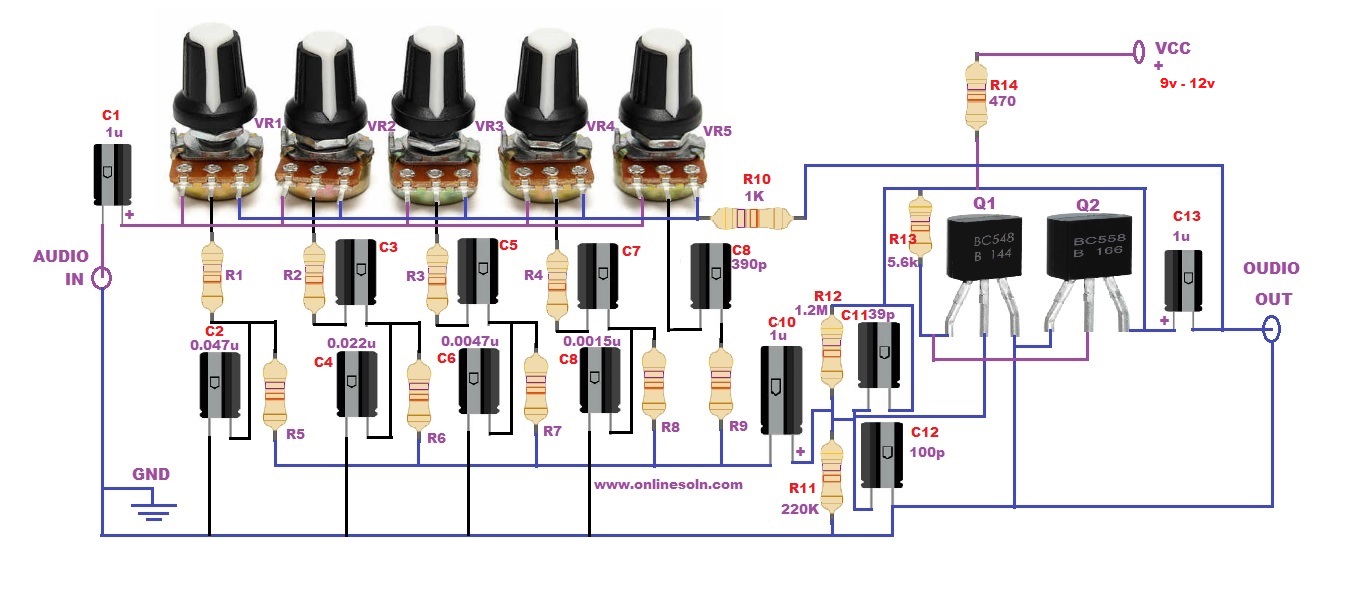
Transistors Graphic equalizer circuit
This equalizer circuit can be adjusted the frequency to 5 channel is 60 Hz, 100 Hz, 1 kHz, 3 kHz, and 12 kHz.
And, this project consists of stereos, right and left channel. It is the same. So, we will learn only the right channel (Mono).
In-circuit is Mono. If you want stereo. Just You add Mono another one only.
I want you to understand easier. Seeing block diagram may you more.
When we enter a signal to the input. Then, C1 passes a signal to couplingthrough pin1 each potentiometer (VR1-VR5).
If we adjust VR5 to a higher level in the middle of a potentiometer.
This signal will come to a high and low-frequency filter of each band. They include the R and C networks.
Next, the signal that through each band be combined together.
Then, C10-capacitor passes the signal to coupling to a base of Q1 and Q2.
Both transistors are a common emitter amplifier.
The higher signal goes out of a collector of Q1. It is out of phase with the input.
Then, the highest signal or the output signal comes out of the emitter of Q2 via C13.
And, some signal will be feedback through R10 to each leg 3 of the potentiometer (VR1 to VR5).
When we adjust them to this point. A feedback signal will refute with an input. So, this is a cut-off point.
How to builds this project
First, find the components of this project. See the parts lists below.
Parts you will need
- 0.25W Resistors, tolerance: 5%
- R1, R2, R3, R4: 22K
- R5, R6, R7, R8, R9: 33K
- R12: 1.2M
- R11: 220K
- R10: 1K
- R13: 5.6K
- R14: 470 ohms
- VR1-VR5: 50K(B) stereo potentiometer
Capacitors
- C1,C10,C13: 1uF 50V Electrolytic
- C2: 0.047uF 50V Mylar
- C3, C4: 0.022uF 50V Mylar
- C5,C6: 0.0047uF 50V Mylar
- C7, C8: 0.0015uF 50V Mylar
- C9: 390pF 50V Ceramic
- C11: 39pF 50V Ceramic
- C12: 100pF 50V Ceramic
Semiconductors
- Q1: BC549 or BC548 Transistors
- Q2: BC558 or BC557 Transistors

Printed circuit board is the most common name but may also be called "printed wiring boards" or "printed wiring cards". Before the advent of the PCB circuits were constructed through a laborious process of point-to-point wiring. This led to frequent failures at wire junctions and short circuits when wire insulation began to age and crack. PCBONLINE